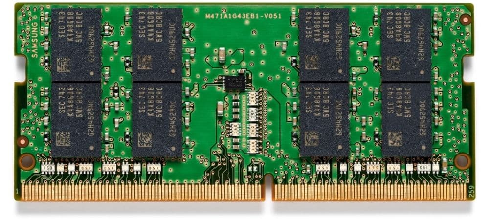
The Random Access Memory, or RAM, of a computer plays a quintessential part in allowing the computer to execute processes and programs. Unlike its counterpart, the ROM (Read Only Memory), the RAM’s memory is actually not permanent or volatile in proper terms. Hence, once the computer is shut down, the contents of the RAM will cease to exist. Therefore, the RAM is not used to store permanent information like the OS program, Input/Output systems, and other necessary utilities. Rather, it acts as the temporary space where the CPU can execute its computations and run your programs or games. This is why most gamers care less about the storage size of ROMs and more often emphasize the RAM when discussing gaming computers.
There are also two primary types of RAM in existence today, namely the Dynamic (DRAM) and Static (SRAM) RAM, with their own specific uses. Of course, this was not the case back in the day. In fact, the RAM has evolved and gone through many different iterations that have upgraded its power and simplified its structure into the minuscule yet complex hardware we know RAM of today. So, let’s take a look at the full history of the RAM, from its initial invention to the recently released state-of-the-art DDR5.
But before that, you will need some basic understanding of the job of RAMs in the computer. For RAMs to work, it needs to be able to read and write information. In other words, we must be able to store information and give that information back to the computer. The reason why we keep getting new iterations of RAM is to speed up each of these two operations. Simple enough? With that out of the way, let’s proceed.
Drum Memory
The first resemblance of a RAM was called Drum memory, invented in 1932 by Gusta Tauschek. Technically speaking, a Drum memory does not fully function as a modern-day RAM and is much more suited to be an HDD or hard disk drive. However, in those olden times, there was no reason to separate the main working memory or secondary memory, which is why we still could consider a Drum memory to be the first generation of RAM.
So how does this ancient technology work? A drum memory’s outside surface is coated using a ferromagnetic material, which acts as the storage that saves binary information. Think of it as a disk or but 100 times larger. There are also read-write heads are positioned above the ferromagnetic surface to input or extract information. If you want to write information into the drum memory, an electromagnetic pulse is produced and the orientation of the magnetic particle in the surface is altered to store the binary information. If we want to perform a read, we can simply scan the intricate orientation of each magnetic particle along the surface. This is as simple as it gets when dealing with a Drum memory.
However, to optimize read-write speeds, we must have a great deal of knowledge of the structure of each hardware component. Programmers, in particular, were constrained to optimum programming, where they strictly position their code in the drum to minimize instruction loading time (also known as skip factor or interleaving). Despite all of these difficulties, drum memory was the primary choice of computer memory for more than two decades since the 1950s due to its efficient memory retrieval and low costs.
Vacuum Tube Memory
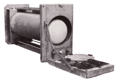
As mentioned previously, Drum memory acts much closer to a disk rather than a RAM due to its non-volatile nature. Thus, the first true grandfather of the RAM is actually the Williams Tube. The Williams Tube was invented in 1949 by Freddie Williams and Tom Kilburn. It utilizes the same exact technology as first-generation bulky TVs, which is the cathode ray tube. The memory writing works by sending an electron beam, deflecting it off with positively charged coils, and striking the phosphor surface to make the grid patterns shown below.
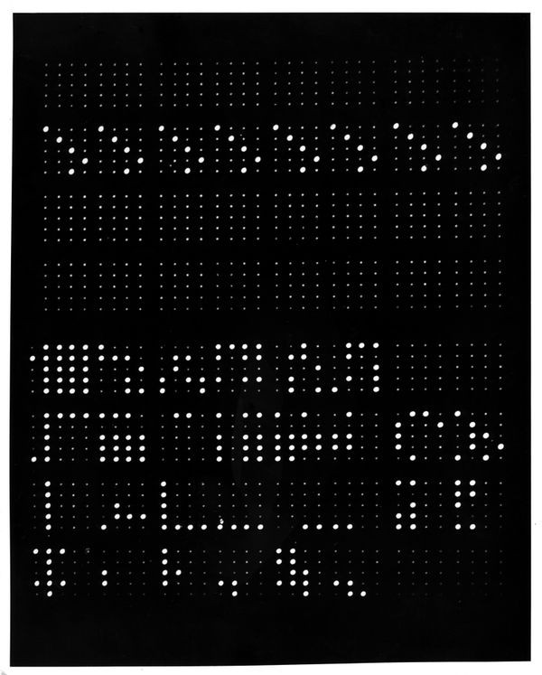
These patterns represent the binary information that can be read by the computer. Like modern-day RAMs, the Williams Tube is non-volatile since these patterns will fade over time and the electron beams can overlap read-writes in each pattern spot. However, the Williams Tube’s major flaw lies in the electron beam deflection process, which is highly sensitive to nearby electrical fields. If there are any charge imbalances surrounding the cathode ray tubes, write operations can severely be compromised. The Vacuum Tube memory was first implemented on the Manchester Baby computer, allowing the computer to successfully run programs in June 1948.
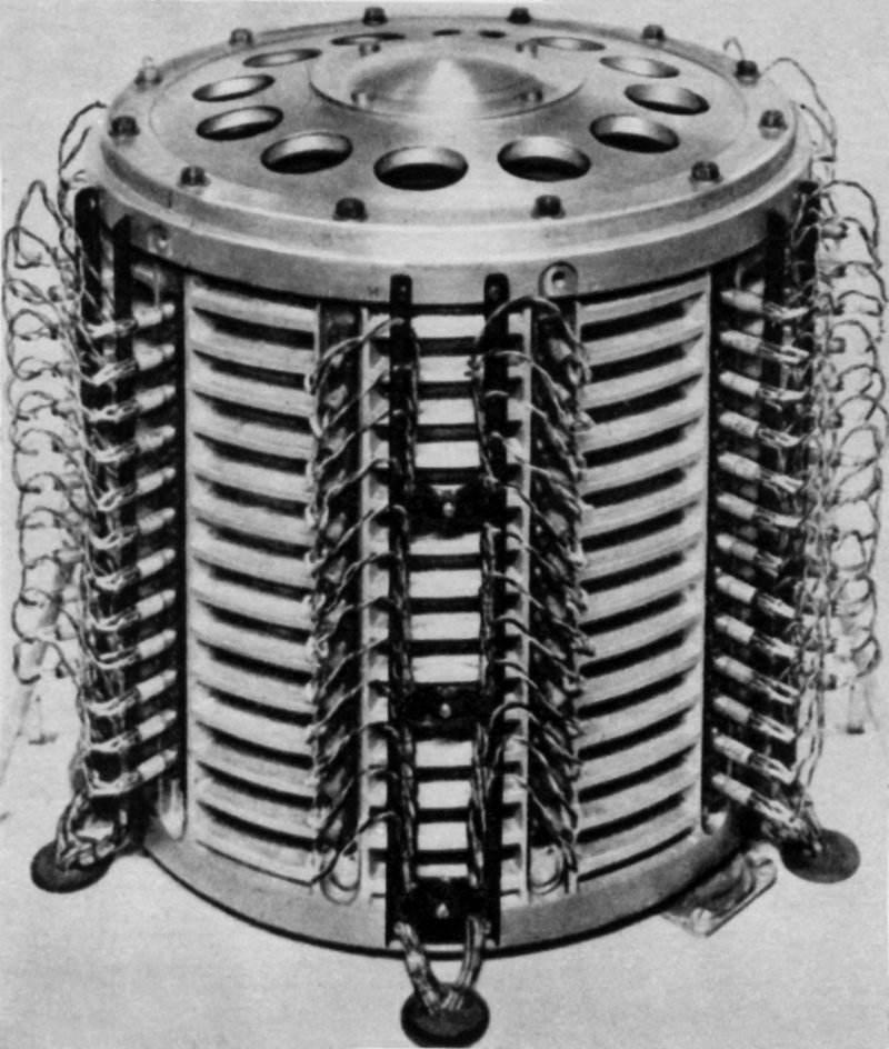
Magnetic Core Memory
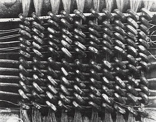
The Magnetic Core memory was considered the commercial RAM for computers in the 1950s up to the 1970s, essentially displacing the use of Drum memory for random-access purposes. The hardware is comprised of many magnetic rings (or core), which can store information due to a phenomenon called Magnetic Hysteresis. Simply put, these rings can remember information by altering the direction of the magnetization. We can change the polarization of these magnets (or input information) by conducting an electrical current to the many wires that run through the rings. As for the read operation, there is a special sensing wire to detect the charge state of each core extract the corresponding binary data.
Before the meta-defining transistors became the norm, these humongous magnetic core memory was the only solution for random access. However, you might be surprised that core memory is actually non-volatile, unlike a normal RAM. Instead, it falls into the category with which we know today as NVRAM. Core memory is able to retain information when the computer is shut-down because the magnetic rings can maintain their polarization.
Static Random Access Memory
Things took a turn after the invention of the metal-oxide-semiconductor or MOS memory in 1964. In short, MOS Memory was able to significantly outperform magnetic core memory while consuming less power and being cheaper to produce. Most importantly, however, MOS memory was able to be shrunk down into small chips that can easily be fitted inside a computer. It quickly took over the market and drove core memory out of fashion
Following the development of MOS, Robert H. Horman invented the first static random-access memory (SRAM) in 1963. A year later the MOS SRAM was invented by John Schmidt. IBM finally utilized SRAMs commercially when they released the SP95 memory chip in 1965.
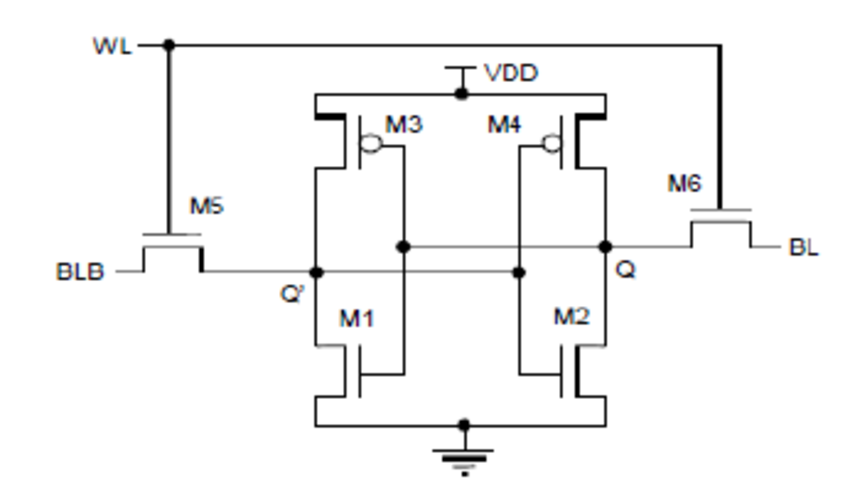
It is not really easy to explain how an SRAM operates since you will require some degree of knowledge in electrical physics. In any case, the most important thing to note here is that SRAMs typically use 6 (MOSFET) transistors to store a bit of memory (either a 0 or 1). You can supply an electrical current accordingly to charge up these transistors and store the binary information, which will stay persistent when supplied with power. The term Static comes from the fact that it does not have to be recharged or refreshed periodically, opposite its counterpart DRAM. Consequently, SRAMs also consume much less power and are used to store more persistent data such as caches or registers that require brief but fast access times.
You might already realize that SRAM is not the RAM that you are probably thinking about. If you are taking a look at computer specs and see the RAM details, that is referring to DRAM. SRAMs also do not get the same amount of attention or development as DRAMs, since it plays a less significant factor in increasing computing power. Furthermore, SRAMs are much more expensive and take up a great deal of space compared to DRAMs. The history of the SRAM’s development is also expectedly boring. For instance, the latest iteration of SRAM was released by Hyundai in 1995 and still uses the same exact same MOSFET technology that was created 3 decades prior.
Dynamic Random Access Memory
We can now discuss the nitty-gritty part of the topic, DRAMs. As mentioned previously, DRAMs are what we would describe today as RAMs. It functions as the main memory for most computers and provides the required space for programs codes to run properly. This is why DRAMs are more important when talking about PC specifications, as it essentially plays a significant part in affecting a computer’s processing power.
So what distinguishes DRAMs from SRAMs? And why can’t they both switch up their jobs on a computer? The answer lies in the structure of both hardware. While SRAMs mostly use 6 transistors to store one bit of information, DRAMs are able to only use 1. Therefore, DRAMs, by their design, are much smaller have a greater storage density. Its relatively simple structure also makes DRAMs much cheaper per bit compared to SRAMs.
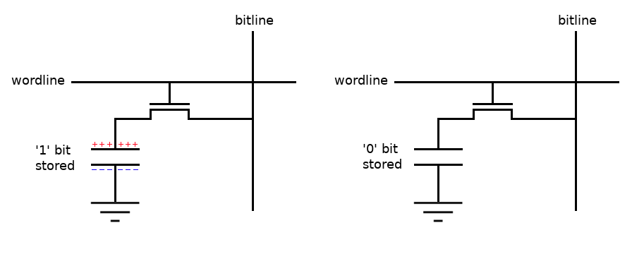
Instead of using 5 extra transistors, DRAMs utilize capacitors to store the information. Capacitors are similar to rechargeable batteries. If the capacitor is charged, it means that it stores a 1. If it is uncharged, it stores a 0. The main caveat of DRAM’s design is that they must be periodically refreshed (hence the dynamic name) to retain information since capacitors slowly leak their charge away. This is the reason why SRAMs are more power-efficient in the long run. However,
The idea for creating DRAMs initially came up in 1966 when Robert H. Dennard was working on the SRAM technology. Dennard realized that a capacitor can be created using the same MOS technology and use transistors it up. And thus, DRAMs were born. The new memory technology was commercialized in 1969 by Honeywell, and, at this point, DRAMs were able to store 1000 bits or 1kbit of data. Unfortunately, this iteration of the DRAM, called 1102, had many problems that didn’t appeal to the market. Intel, which previously worked with Honeywell, eventually redesigned the DRAM and created a brand new chip on their own, called 1103. This was the first DRAM chip that was truly commercially ready and available for the public.
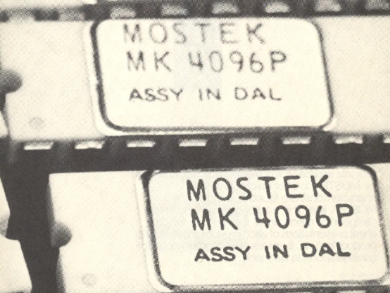
DRAM technology was upgraded in 1973 when Mostek released its MK4096 4000-bit chip. Designed by Robert Proebsting, the new DRAM made a significant breakthrough by utilizing an effective multiplexed addressing scheme. Essentially, this new design uses single address pins to access memory rows and columns by doing it in turn. In previous DRAMs, you would have to do this with two pins and address lines. Of course, reducing the number of pins also drops significantly down manufacturing costs, especially when memory size and density grow larger.
Mostek released the second iteration of its new DRAM chip called the MK4116, this time having 16 kbit of storage. The MK4116 chip proved to be very popular in those times and managed to own 3 quarters of the worldwide DRAM market share at one point. The last commercially produced chip was made by Samsung in February of 2001 with a capacity of 4 Gbit, and that seals the deal with the DRAM era.
But, of course, the RAM story did not end in 2001. Instead, it marked a transition towards a more advanced type of RAM called synchronous dynamic random-access memory or SDRAM.
Synchronous Dynamic Random Access memory
The primary difference between SDRAM and DRAM lies in their names. Regular DRAMs operate asynchronously with respect to the computer’s system clock, while SDRAMs will always stay synchronized. As a result, read-write operations of SDRAM are far more efficient and fast compared to DRAMs. The memory structure of SDRAM is also divided into a number of memory banks that allow for concurrent accesses, which improves speed yet again.
Samsung coincidentally was also the first manufacturer of the SDRAM chip called KM48L2000, which has a measly capacity of 16 Mbit. In June 1998, Samsung began experimenting with the DDR or Double Data Rate technology. DDR essentially allows data transfers to occur twice as fast compared to normal SDRAMs since it is able to send or receive signals two times per clock cycle. 3 years later, DDR2 was created, which doubles the speed of DDR1 yet again since it performs access four times per clock cycle. At this point, however, most large RAM manufacturers out like Sony and Toshiba there haven’t jumped into the DDR hype train, putting more effort into producing embedded DRAMs or eDRAMs.
DDR3 was eventually developed in 2003 by, you guessed it, Samsung. Again, DDR3 doubled the read-write rate to 8 accesses per cycle. Despite all the increase in speeds, its progress is still heavily held back with latency or most commonly known as CAS latency. CAS Latency pertains to the delay between the RAM in responding to data access requests and, obviously, the lower latency the better. Unfortunately, the CAS latency increases as we continue to double our data rate, which means that slower SDRAMs might have a marginally lower “true” latency (latency that we experience).
Unlike the previous iterations of DDR, DDR3 gained widespread adoption by manufacturers and by the general users as well. Starting from mid-2008, Samsung began to commercialize DDR3 chips, initially with a capacity of 8192 Mbit. The chips were a massive hit and many computer systems in that time begin opting to use the DDR technology. Consequently, Samsung continued to upgrade the capacity and clock rates of the DDR3 to combat the aforementioned problem of latency. Another relatively new player in the RAM manufacturing business also began to jump into the DDR3 fray called SK Hynix. Both the Korean tech companies create the necessary competitiveness in the market to constantly improve the DDR3 technology to the next level.
Information about DDR4 was teased at Intel Developer Forum in 2008, which was expected to be released in 2011. Hynix struck first and released a DDR4 prototype in early 2011 with a capacity of 2048. The new double data rate tech promised a lot of things, lower power consumption (1.2v compared to 1.5v) and faster data transfers just to name a few. Samsung eventually commercialized its DDR4 chip in 2013, but most people have grown accustomed to its predecessor DDR3. Thus, the DDR4 technology only gained widespread adoption later in 2015.
As for the latest iteration of the DDRAM, we have DDR5. The JEDEC standards of DDR5 were already significantly delayed by 2 years after its initial expected release in 2018. Many manufacturers have also begun laying down their plans to release their DDR5 chips, some even already have put them out on the market for purchase.
However, you should probably not get your hands on a DDR5 as of now. Indeed, like all DDRAM updates, there is always a speed or performance gain. DDR5 also further decreases the memory voltage down to 1.1v compared to the 1.2v of the DDR4. Despite all these merits, DDR5s are probably not stable or compatible with most hardware or processors out there. The price of this new RAM also speaks for itself. DDR4, despite being more than 7 years old, is probably still the most suitable RAM to use as of now.
Conclusion
The DDR5 marks end of the history of the Random Access Memory, one of the most sought-after hardware components when discussing computing speed. If we take a look back again at the progress of the RAM, we were able to shrink giant-like magnetic core structures that used to fill up a whole room into minuscule pocket-sized hardware while exponentially increasing its storage capacity and access effectivity. That right just goes to show another feat of human intelligence and the immense power it beholds.
Featured Image: Freepik